English


| Specifications | Details |
|---|---|
| CL(IDD) | 22 cycles |
| Row Cycle Time (tRCmin) | 45.75ns (min.) |
| Refresh to Active/Refresh | 350ns (min.) |
| Command Time (tRFCmin) | |
| Row Active Time (tRASmin) | 32ns (min.) |
| Maximum Operating Power | TBD W* (*Power will vary depending on the SDRAM used.) |
| UL Rating | 94 V – 0 |
| Operating Temperature | 0°C to +85°C |
| Main Chips | Micron, Samsung, Hynix |
| Storage Temperature | -55°C to +100°C |
| Description | Details |
|---|---|
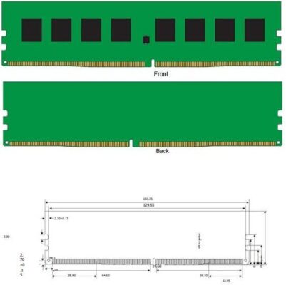
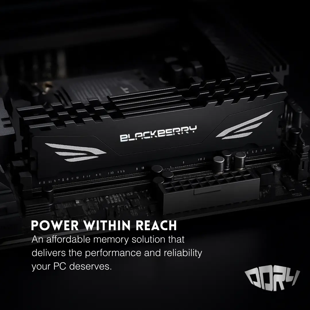
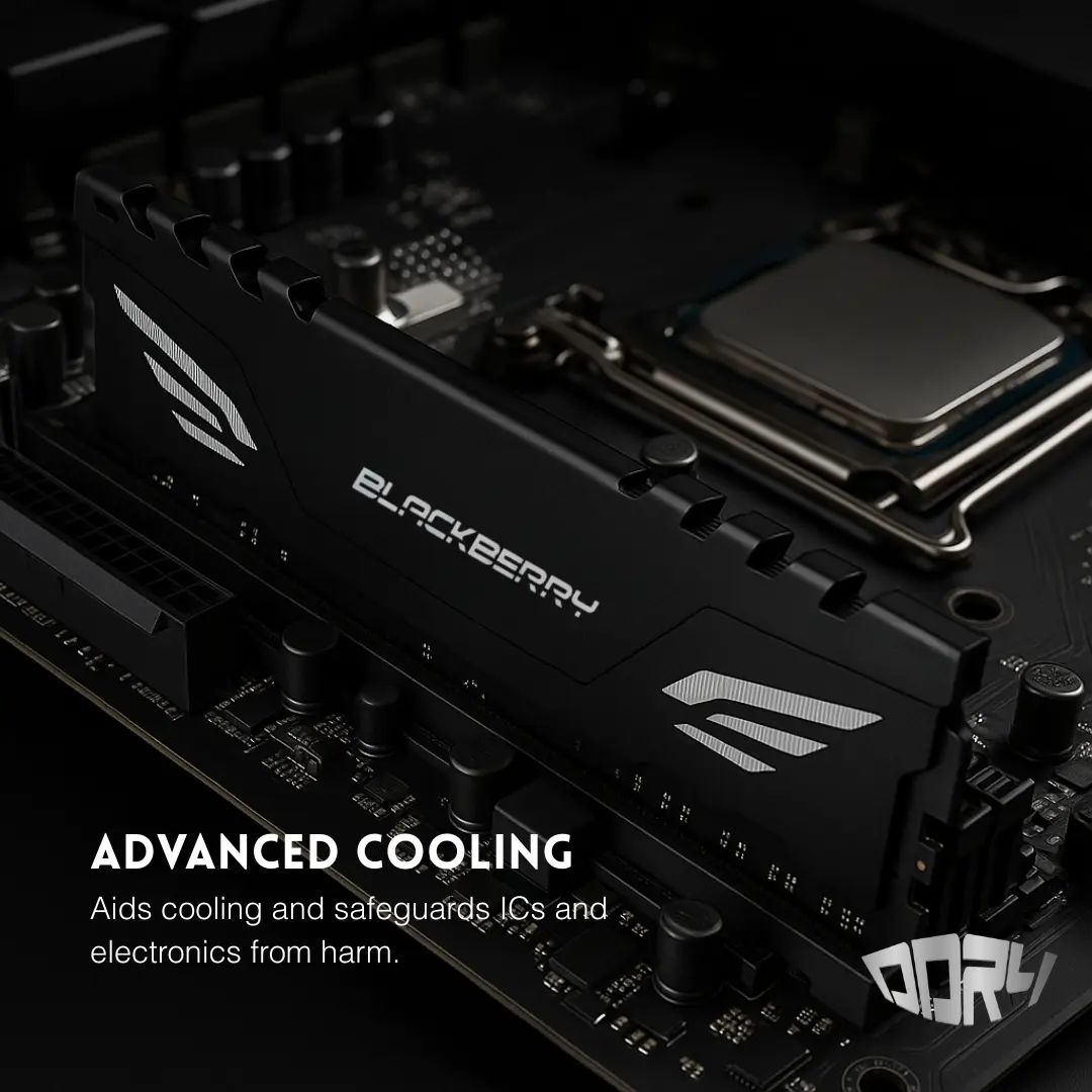
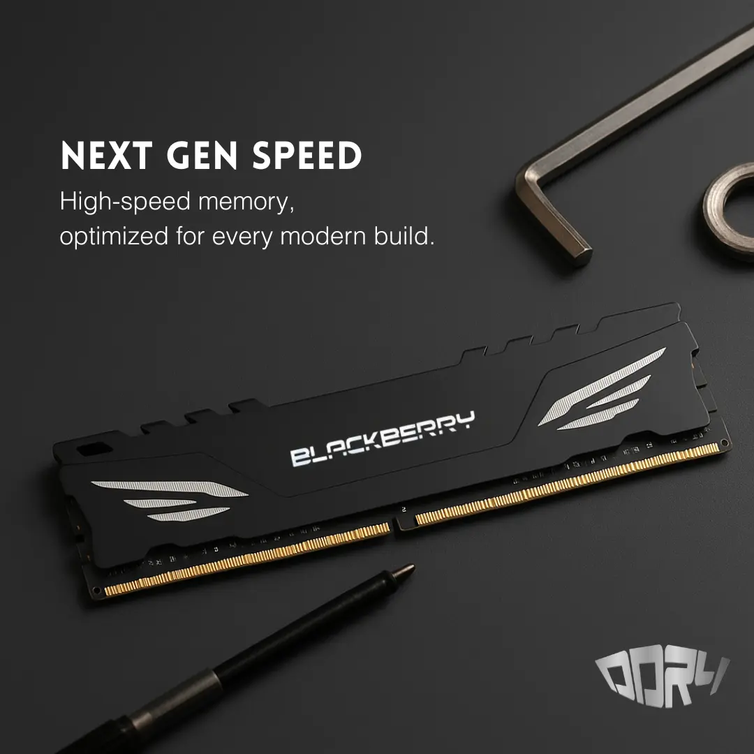
| Description | This document describes Value RAM is a 1G x 64-bit (8GB) DDR4-3200 CL22 SDRAM (Synchronous DRAM), 1Rx8, memory module, based on eight 1G x 8-bit FBGA components. The SPD is programmed to JEDEC standard latency DDR4-3200 timing of 22-22-22 at 1.2V. Each 288-pin DIMM uses gold contact fingers. The electrical and mechanical specifications are as follows. |
| Features | Details |
|---|---|
| Power Supply | VDD=1.2V Typical |
| VDDQ | 1.2V Typical |
| VPP | 2.5V Typical |
| VDDSPD | 2.2V to 3.6V |
| Nominal and dynamic on-die termination (ODT) for data, strobe, and mask signals | |
| Low-power auto self refresh (LPASR) | |
| Data bus inversion (DBI) for data bus | |
| On-die VREFDQ generation and calibration | |
| Single-rank | |
| On-board I2 serial presence-detect (SPD) EEPROM | |
| 16 internal banks; 4 groups of 4 banks each | |
| Fixed burst chop (BC) of 4 and burst length (BL) of 8 via the mode register set (MRS) | |
| Selectable BC4 or BL8 on-the-fly (OTF) | |
| Fly-by topology | |
| Terminated control command and address bus | |
| PCB | Height 1.23” (31.25mm) |
| RoHS Compliance | Compliant and Halogen-Free |